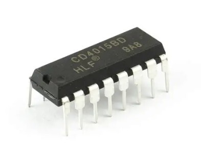
CD4015 SHIFT REGISTER
Share :
The CD4015 is a versatile CMOS integrated circuit (IC) that is a Dual 4-Stage Static Shift Register with Serial Input and Parallel Output (SIPO).
This means it contains two separate, identical 4-bit shift registers within a single package.
Here's a breakdown of its key functions, features, and applications:
Serial-to-Parallel Data Conversion: The primary function is to take data one bit at a time (serially) and make all 4 bits available simultaneously (in parallel) at the output pins.
Data Shifting and Storage: It uses D-type master-slave flip-flops to store and shift the data. On each positive-going clock transition (rising edge of the clock pulse), the logic level present at the data input is shifted into the first stage, and the data in all subsequent stages shifts one position down the register.
I/O Expansion: It is commonly used with microcontrollers (like Arduino) to expand the number of output pins available, allowing a small number of microcontroller pins (Clock, Data, and Reset) to control many outputs (e.g., LEDs, LCD segments).
| Feature | Description |
| Registers | Two independent, 4-stage shift registers. |
| Inputs per Register | Independent Data (D), Clock (CLK), and Reset (RST) inputs. |
| Outputs per Register | 4 parallel outputs (Q_1, Q_2, Q_3, Q_4). |
| Logic Type | CMOS (Complementary Metal-Oxide-Semiconductor) - known for low power consumption. |
| Operating Voltage | Wide range, typically 3V to 18V. |
| Reset | A logic HIGH on the Reset pin clears all four stages of that register (sets all outputs to LOW). The Reset pin is typically held LOW for normal shifting operation. |
| Cascading | The two 4-bit registers can be easily connected (cascaded) to form a single 8-bit shift register, and multiple ICs can be cascaded for even longer registers. |
| Pin Name | Pin # | Function |
| Clock B (CLKB) | 1 | Clock input for Register B. |
| Q_4B, Q_3B, Q_2B, Q_1B | 2, 13, 12, 11 | Parallel outputs for Register B. |
| Q_3A, Q_2A, Q_1A | 3, 4, 5 | Parallel outputs for Register A (Note: non-sequential pin numbering). |
| Reset A (RSTA) | 6 | Reset input for Register A (active HIGH). |
| Data A (DA) | 7 | Serial Data input for Register A. |
| Ground (V_SS) | 8 | Connect to the negative power supply/ground. |
| Clock A (CLKA) | 9 | Clock input for Register A. |
| Q_4A | 10 | Parallel output for Register A. |
| Reset B (RSTB) | 14 | Reset input for Register B (active HIGH). |
| Data B (DB) | 15 | Serial Data input for Register B. |
| Supply Voltage (V_DD) | 16 | Connect to the positive power supply. |
LED Chaser/Running Light Circuits: Used to sequentially turn LEDs on and off, controlling a string of lights.
Microcontroller I/O Expansion: Increasing the number of output pins from a microcontroller to drive more peripherals.
Data Queueing: Temporarily storing and managing a sequence of data bits.
Data Multiplexing/Demultiplexing (in conjunction with other components).

