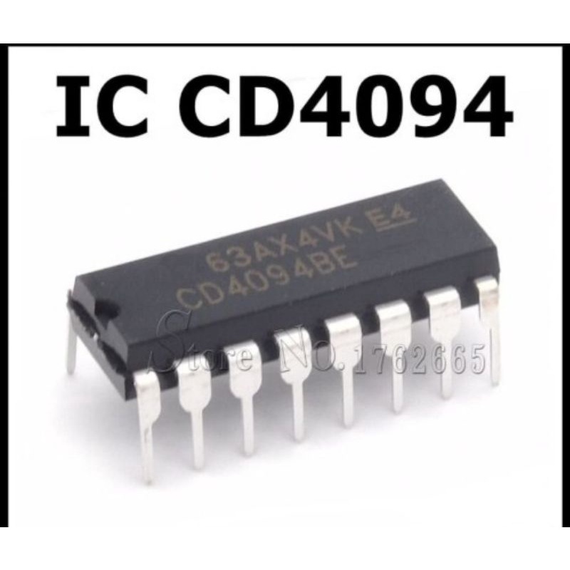
CD4094
Share :
The CD4094 is an integrated circuit (IC) that functions as an 8-stage serial shift register with an 8-bit storage latch and 3-state parallel outputs. It is a CMOS device and is often referred to as an 8-Stage Shift-and-Store Bus Register.
Key Functions and Features
Serial-to-Parallel Data Conversion: Its primary purpose is to convert serial data (a stream of single bits) into parallel data (8 bits simultaneously) for driving multiple outputs.
8-Bit Shift Register: Data is entered serially at the DATA input and is shifted one position down the register on the positive transition of the CLOCK input.
8-Bit Storage Latch: The data in the shift register is transferred to an internal storage register (latch) when the STROBE input is high. This allows the outputs to be updated only when the entire 8 bits have been shifted in.
3-State Parallel Outputs (Q1-Q8): The outputs can be connected directly to a common bus line and are controlled by the OUTPUT ENABLE pin. When OUTPUT ENABLE is high, the data from the storage latch appears at the outputs. When OUTPUT ENABLE is low, the outputs go into a high-impedance (3-state) OFF-state.
Cascading: The IC includes two serial outputs, QS and Q'S, which enable multiple CD4094 devices to be chained together for applications requiring more than 8 bits of shift-and-store capability.
CMOS Technology: It features a wide supply voltage range (typically 3.0V to 18V) and offers high noise immunity and low power consumption.
Common Applications
Expanding Microcontroller Outputs: It is frequently used with microcontrollers to control multiple LEDs or other devices, saving precious microcontroller I/O pins.
Serial-to-Parallel Data Conversion: Useful in digital systems for changing data format.
Remote Control Holding Register: Storing data for various control applications.
This video provides an explanation of the CD4094's operation and demonstrates its use: CD4094 IC Explained: How to Use This 8-Bit Shift Register!.

